Technology
Thin Film Coating (Vacuum Deposition /Sputtering)
Additional performance to optical parts
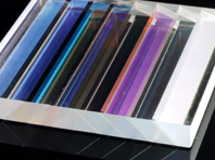
Thin film coating is the process of coating glass and crystal, etc. It is to coat substrates with metal and semi-conducting materials, dielectric substances (metal oxides, fluorides, etc.) using vacuum deposition, sputtering techniques and vapor growth methods, etc. These coatings will add characteristics and functions to glass for reflection, transmission, absorption, emission, refraction, interference and diffraction, etc. from extreme ultraviolet, visible to infrared wavelength ranges. Thin film can be coated with more than 100 layers depending on the specifications.
The history of thin film coating in NITTO OPTICAL begins with AR coatings, enhanced aluminum reflection coatings and ITO film (transparent conducting layers), followed by the handling of demultiplexing film, wavelength separation film. Now NITTO OPTICAL has established coating technology for dielectric multilayer film.
Capable wavelength ranges from optical parts (ArF: 193nm) for semiconductor exposure devices to optical components (1.55 micron belt) for fiber optics. NITTO OPTICAL has been under research and development for EUV (extreme ultraviolet beam) wavelength band and multi-wavelengths for the next generation. Some of the R & D results have been announced at exhibitions, etc.
To satisfy the customers coating requirements from a wide variety of markets, NITTO OPTICAL uses the most appropriate devices for customer specifications and adds the original technology to the IAD (Ion Assisted Deposition) and magnetron-sputtering, etc for thin film. These approaches provide the stable quality from prototypes for research and development up to mass production.
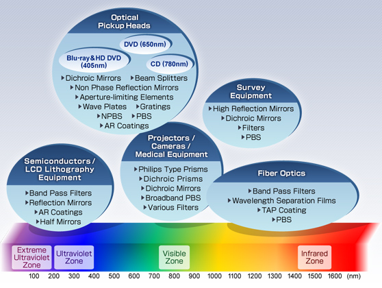
Handling various wavelength ranges
NITTO OPTICAL satisfies customer coating requirements in various wavelength ranges, beginning from the coating simulation.