Micro-Patterning / Bonding / Cutting / Cleaning
Technology supporting microfabrication and integrated mass production system
Micro-Patterning
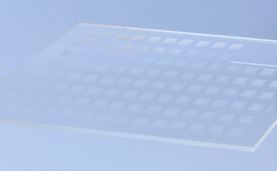
Micro-patterning is a processing technology that forms fine structures on glass or semiconductor substrates, and it is an essential process for manufacturing optical elements and electronic devices. In particular, photolithography is widely used as a technique for forming precise patterns using photosensitive materials (photoresist).
NITTO OPTICAL has developed its own processes in dry and wet etching technologies, and realizes high-precision patterning.
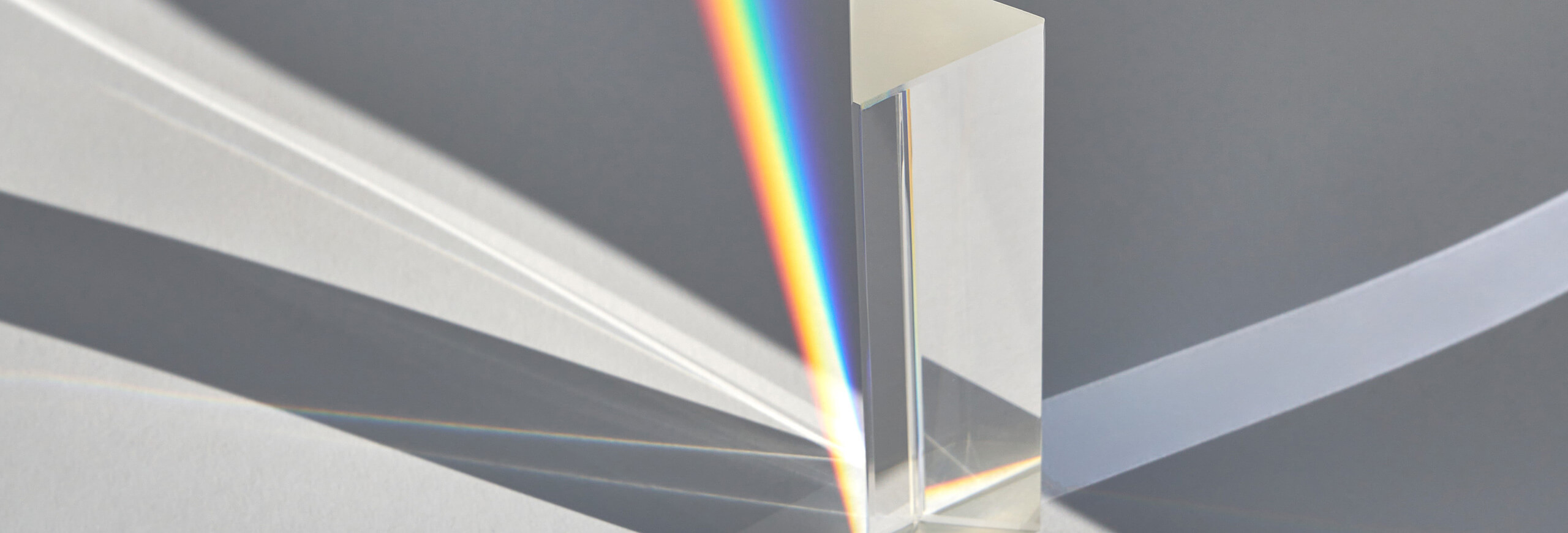
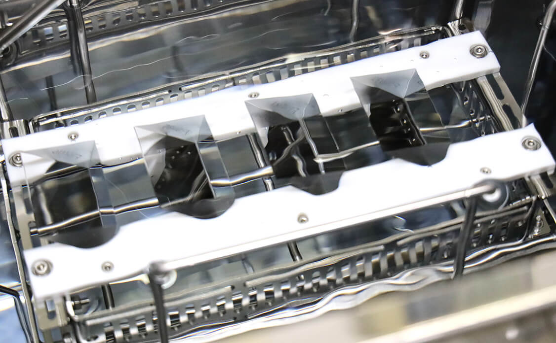
Bonding / Adhesion
Specification, which cannot be satisfied in single prism, can be met by bonding prisms. The adhesion of metal/plastic parts to prisms is also being cured according to customer requirements.
NITTO OPTICAL selects adhesives suitable for the material and product specification. NITTO OPTICAL measures the beam deviation accuracy and spectral characteristics with measuring instruments.
For laser diodes and high-power lasers (YAG lasers, excimer lasers etc.), NITTO OPTICAL has optical contact technology without using adhesives to bond prisms with extreme high flatness.
Cutting
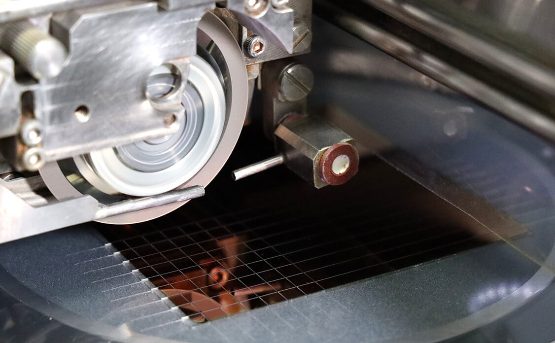
NITTO OPTICAL has various dicers, slicers, and inner blade cutting machines, etc., to satisfy requirements, regardless of quantity, size, prototype and mass production.
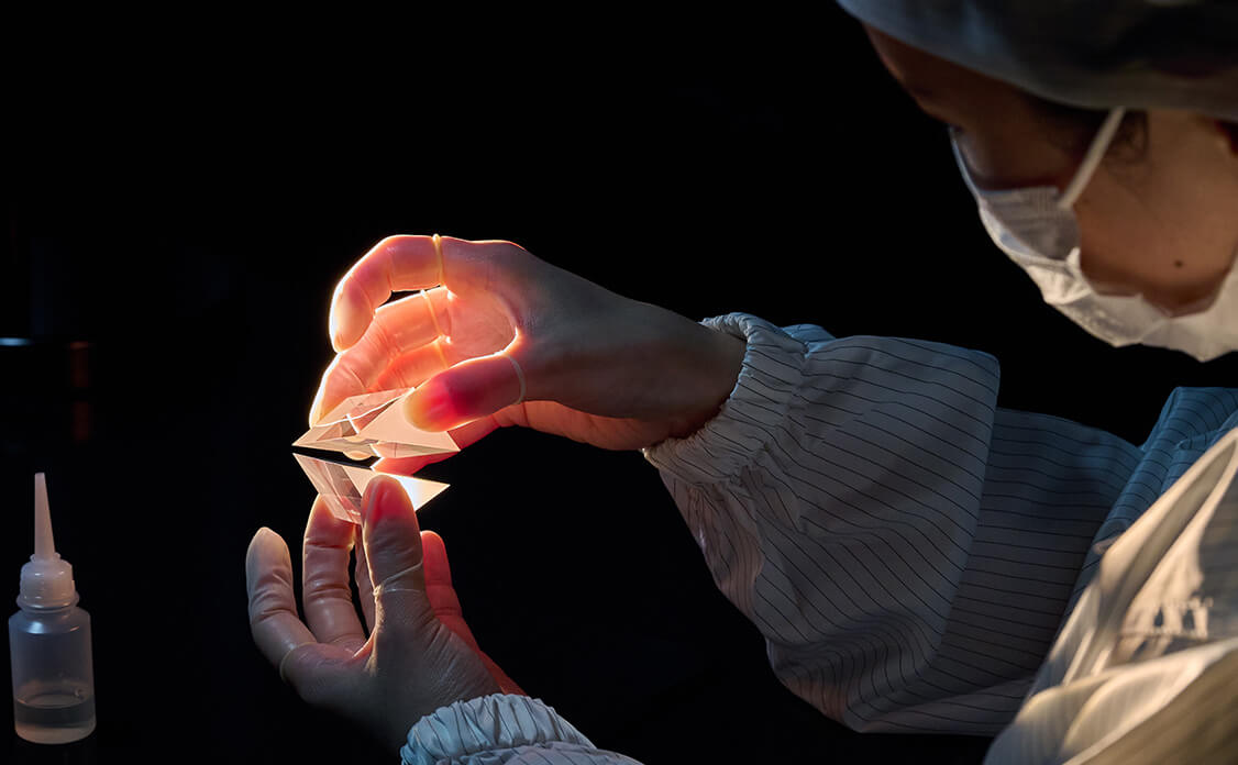
Cleaning
The point of the cleaning process is to remove residue such as glass particles, grinding fluid and polishing agents, etc. and organic dirt that stick to optical parts generated in the grinding/ polishing process to improve following thin film coating process.
Product dirt (contamination) is removed by multi-layer ultrasonic cleaning machines in each step of grinding/polishing and thin film coating (vacuum deposition and sputtering).